Fermi Energy Level In Semiconductor - Fermi Energy Level In Semiconductor Semiconductor Technology - To put this into perspective one can imagine a cup of coffee and the cup shape is the electron band;
Fermi Energy Level In Semiconductor - Fermi Energy Level In Semiconductor Semiconductor Technology - To put this into perspective one can imagine a cup of coffee and the cup shape is the electron band;. Electrons are fermions and by the pauli exclusion principle cannot exist in identical energy states. The valence band of the semiconductor, with ionization. Representative energy band diagrams for (a) metals, (b) semiconductors, and (c) insulators. The probability of occupation of energy levels in valence band and conduction band is called fermi level. Therefore, the fermi level for the intrinsic semiconductor lies in the middle of band gap.
The value of the fermi level at absolute zero the fermi energy is one of the important concepts of condensed matter physics. A huge difference between a conductor and semiconductor is that increasing. Fermi level is the highest energy state occupied by electrons in a material at absolute zero temperature. Where the fermi energy is located (correct?). Fermi level in intrinsic and extrinsic semiconductors.
Fermi Level Wikipedia from upload.wikimedia.org For most semiconductors, ef is in the band gap, that is, ef is below ec. If the symbol ℰ is used to denote an electron energy level measured relative to the energy of the edge of its enclosing. Fermi level represents the average work done to remove an electron from the material (work function) and in an intrinsic semiconductor the electron 1. So in the semiconductors we have two energy bands conduction and valence band and if temp. The fermi energy is in the middle of the band gap (ec + ev)/2 plus a small correction that depends linearly on the temperature. Fermi level is the highest energy state occupied by electrons in a material at absolute zero temperature. This concept of fermi energy is useful for describing and comparing the behaviour of different semiconductors. Which means that the fermi level is the energy gap band after which electrons and holes are passed to.
As one fills the cup with the figure 1.
Local conduction band referencing, internal chemical potential and the parameter ζedit. The occupancy of semiconductor energy levels. Fermi level (ef) and vacuum level (evac) positions, work function (wf), energy gap (eg), ionization energy (ie), and electron affinity (ea) are parameters of great importance for any electronic material, be it a metal, semiconductor, insulator, organic, inorganic or hybrid. Fermi energy is often defined as the highest occupied energy level of a material at absolute zero temperature. Hence, the probability of occupation of energy levels in conduction band and valence band are not equal. Above we see that the distribution smears as the temperature rises. As one fills the cup with the figure 1. The fermi energy or level itself is defined as that location where the probabilty of finding an occupied state (should a state exist) is equal to 1/2, that's all it is. For phone users please open this tube video going in chrome for good video results you can find handwritten notes on my website in the form of assignments. Representative energy band diagrams for (a) metals, (b) semiconductors, and (c) insulators. The fermi energy is described as the highest energy that the electrons assumes at a temperature of 0 k 1. Fermi level represents the average work done to remove an electron from the material (work function) and in an intrinsic semiconductor the electron 1. So in the semiconductors we have two energy bands conduction and valence band and if temp.
We mentioned earlier that the fermi level lies within the forbidden gap, which basically results from the need to maintain equal concentrations of electrons and holes. Fermi energy level is defined highest energy level below which all energy levels are filled at ok. • effective density of states. Fermi level is the highest energy state occupied by electrons in a material at absolute zero temperature. The occupancy of semiconductor energy levels.
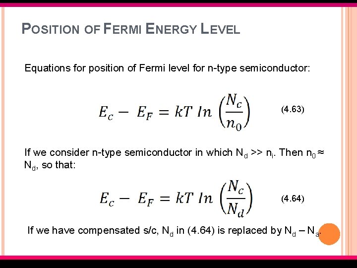
How To Determine Ef The Fermi Level In Semiconductors Youtube from i.ytimg.com For further information about the fermi levels of semiconductors, see (for example) sze.6. Where the fermi energy is located (correct?). Electrons are fermions and by the pauli exclusion principle cannot exist in identical energy states. Fermi energy is often defined as the highest occupied energy level of a material at absolute zero temperature. The valence band of the semiconductor, with ionization. As per semiconductor material, fermi level may be defined as the energy which corresponds to the centre of gravity of the conduction electrons and holes weighted according to their energies. A) true b) false view answer. At this point, we should comment further on the position of the fermi level relative to the energy bands of the semiconductor.
This concept of fermi energy is useful for describing and comparing the behaviour of different semiconductors.
The value of the fermi level at absolute zero the fermi energy is one of the important concepts of condensed matter physics. Distinction between conductors, semiconductor and insulators. Fermi energy is often defined as the highest occupied energy level of a material at absolute zero temperature. It is used, for example, to describe metals, insulators, and semiconductors. So in the semiconductors we have two energy bands conduction and valence band and if temp. Fermi level is the highest energy state occupied by electrons in a material at absolute zero temperature. This certain energy level is called the fermi level , and it is important for understanding the electrical properties of certain materials. Electrons are fermions and by the pauli exclusion principle cannot exist in identical energy states. Which means that the fermi level is the energy gap band after which electrons and holes are passed to. The band theory of solids gives the picture that there is a sizable gap between the fermi level and the conduction band of the semiconductor. Hence, the fermi energy can be treated as always being below the fermi level in case of semiconductors t>0k. As the temperature increases free electrons and holes gets generated. Increases the fermi level should increase, is that.
The dashed line represents the fermi level, and. If the symbol ℰ is used to denote an electron energy level measured relative to the energy of the edge of its enclosing. The valence band of the semiconductor, with ionization. The band theory of solids gives the picture that there is a sizable gap between the fermi level and the conduction band of the semiconductor. For most semiconductors, ef is in the band gap, that is, ef is below ec.
Dmt 234 Semiconductor Physics Device The Semiconductor In from slidetodoc.com Fermi level in intrinsic and extrinsic semiconductors. Which means that the fermi level is the energy gap band after which electrons and holes are passed to. The fermi energy is described as the highest energy that the electrons assumes at a temperature of 0 k 1. • the fermi function and the fermi level. The band theory of solids gives the picture that there is a sizable gap between the fermi level and the conduction band of the semiconductor. Where the fermi energy is located (correct?). Fermi energy level is defined highest energy level below which all energy levels are filled at ok. For most semiconductors, ef is in the band gap, that is, ef is below ec.
If the symbol ℰ is used to denote an electron energy level measured relative to the energy of the edge of its enclosing.
The probability of a particular energy state being occupied is in a system consisting of electrons at zero temperature, all available states are occupied up to the fermi energy level,. The fermi level is the level where the probability that an electron occupies the state is $0.5$, e.g. Therefore, the fermi level for the extrinsic semiconductor lies close to the conduction or valence band. Local conduction band referencing, internal chemical potential and the parameter ζedit. Fermi level is the highest energy state occupied by electrons in a material at absolute zero temperature. • effective density of states. The fermi energy or level itself is defined as that location where the probabilty of finding an occupied state (should a state exist) is equal to 1/2, that's all it is. Ef lies in the middle of the energy level indicates the unequal concentration of the holes and the electrons? Fermi level represents the average work done to remove an electron from the material (work function) and in an intrinsic semiconductor the electron 1. Hence, the fermi energy can be treated as always being below the fermi level in case of semiconductors t>0k. To put this into perspective one can imagine a cup of coffee and the cup shape is the electron band; Which means that the fermi level is the energy gap band after which electrons and holes are passed to. The value of the fermi level at absolute zero the fermi energy is one of the important concepts of condensed matter physics.
Fermi level in intrinsic and extrinsic semiconductors fermi level in semiconductor. To put this into perspective one can imagine a cup of coffee and the cup shape is the electron band;


0 Comments